
What makes a truly world-changing invention?. There are many contenders for the most significant invention of the 20th century, the jet engine, the airplane, television, the internet, the computer and antibiotics are all worthy contenders but unless you live like an 15th-century hermit or a part of an undiscovered tribe, there is one which touches the lives of almost everyone on the planet on a daily basis, though few have seen them directly they are now the most widely manufactured device in history.
In 1954 the worlds first transistor radio, the Regency TR-1 used four Texas Instruments npn transistors and cost $49.95 equivalent $507 in 2021. Today, a 512GB SD card can contain over a trillion transistors and costs about $30.
As of 2018 an estimated 13 sextillion, that’s 13 billion, trillion of them have been made since 1960, a number that now grows by thousands of trillions every day and at an increasing rate.
Nothing else made by humans comes even close to the rate of change that the transistor has gone through in just over 60 years and enabled other world-changing technologies and discoveries well beyond the world of electronics.
This is the story of the metal–oxide–semiconductor field-effect transistor or MOSFET and how it changed the world and where might it go in the future.
It could be said that start of the modern world as we know it today began on December 23rd 1947 when the first PNP point-contact germanium transistor was demonstrated to the management of Bell Labs and whilst that might be technically correct, one type of transistor, the MOSFET would enable for the large scale integrated circuits would become the building blocks of the devices that now power the modern world and the device that you are watching this video didn’t arrive until a decade later in 1960.
Now I know that there might be quite a few people out thinking, yea, I’ve heard of transistors but what are they and what do they do?.
A transistor is a basic electronic component and is mostly used in two ways, one is an amplifier the other is as an electronic switch. Now this may seem like two very different functions for the same device but they are really the same, it just depends on how its used in a circuit.
There are many different types of transistors but they have three connections called, emitter, base, collector for Bipolar junction transistors and drain, gate and source for Field Effect Transistors or FETs.
For Bipolar junction transistors, the amount of current fed to the base controls the current flowing between the collector and emitter and in FET’s the amount of voltage applied to the gate controls the current flowing between the drain and source.
In general, applying a carefully controlled amount of current or voltage depending on which type the transistor is, it can work as an amplifier, but apply a larger current or voltage and it will saturate or switch to fully on, remove the current or voltage and it will switch fully off, it’s now working as an electronic switch.
When it’s used in a computer, this switching on and off represents the logical 1’s and 0’s in binary code which is the basic element of all computer programs, and in today’s computer CPU’s they can switch on and off billions of times a second.
Now today, whilst we can see the usefulness of having billions of transistors all working together in modern CPU’s and memory there was a time not long after the transistor had been developed when even the people who made them couldn’t see the point of having so many together. After the first IC to have 10,000 transistors was developed in 1973, one of the executives of a chipmaker was reported to have said “why would anyone need 10,000 transistors in one chip”. One of the first uses for such IC’s was for pocket calculators and the early microprocessors and memory chips.
The first commercially produced microprocessor was the Intel 4004, a 4 bit CPU in 1971 which contained 2500 transistors. Compare that to today’s Apple A15 CPU which powers the iPhone 13, which has 15 billion transistors.
The development of the transistor was a reaction to the thermionic valve or vacuum tube which had been developed in 1907 and had ushered in the first electronic revolution, enabling radio, TV, Radar and eventually the first fully electronic computers.
Although valves are of a completely different design, the triode valve was the equivalent to a transistor, it had three connections, the Plate, Grid and Cathode. A voltage applied to the grid would control the flow of electrons from the cathode to the anode and act as an amplifier or switch depending on how much voltage was applied.
But as good as valves were they had several major drawbacks. They were, with a few later exceptions made from glass and susceptible to breakage from shock and vibrations. They took time to warm up and like light bulbs, they used a filament to create the electron flow but the thermal stress of heating up the filament from cold when switched on was the biggest cause of failures, plus the heater filament also uses a lot of power.
They were also large, even the subminiature versions created for hearing aids and the proximity fuse were much larger than the first commercial transistors. If you were to make a smartphone from valves it would be the size of the Washington monument.
Valves were used in the first radio’s and for amplifying the very small signals from things like the newly developed microphones, these circuits often only needed a handful of valves to work.
Only in the 1940s with the development of the first electronic digital computer, the Colossus at Bletchley Park in England did large numbers of valves start to be used with 2400 valves in the Colossus MkII. By 1946 the ENIAC computer had increased this to 17,000 but this created a new phenomenon called the Tyranny of the numbers.
Basically, the bigger a system like a computer got the more likely it was to break down and the longer it took to troubleshoot and fix.
This was such a problem that the speed increase that was promised by its greater capacity was offset by the downtime it would spend being fixed, something which we will come back to shortly because its key to where we are today.
The Field Effect Transistor or FET was an attempt to eliminate some of these issues to make a solid-state version of a triode valve. This was first patented in 1925 in Canada by Austro-Hungarian physicist Julius Edgar Lilienfeld. Whilst Lilienfeld came up with the idea and proposed how they would work and could be built, the technology of the day was just too primitive for him to build a working prototype.
It was William Shockley working for Bell Labs in the 1940s unsuccessfully trying to build a FET that led John Bardeen, Walter Brattain working under Shockley to discover the transistor effect and by accident, they created the point-contact transistor and then shortly after the first true commercial version, the Bipolar junction transistor which went on to allow their use of the first commercial applications in the transistor radios and TV’s of the late 1950s and early 1960s.
With the creation of the transistor, it was thought that their smaller size and lower power would be a cure to the Tyranny of the numbers but making things smaller didn’t make them more reliable and in many cases just made them more difficult to repair.
As the transistor developed and the main material used to make them changed from Germanium to Silicon which could work over a much great temperature range it was realised that you could make complete circuits on a single piece of silicon consisting of multiple transistors, resistors and even capacitors.
These integrated circuits could be made to do a particular function that before would have used many discrete components and therefore could be much smaller, use less power and be more reliable.
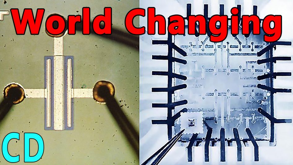
The way Bipolar junction transistors or BJT’s had to be fabricated on the silicon was complicated but several developments in how the silicon was processed led to a breakthrough by Mohamed Atalla and Dawon Kahng at Bell labs in 1959 when they created the first metal–oxide–semiconductor field-effect transistor or MOSFET.
The advantages of the MOSFET had it that they required little or no current to control the load compared to Bipolar junction transistors, they could be much more easily scaled and were easier to mass-produce.
One of the features MOSFET’s were found to have was that if a second electrically isolated gate or a floating gate were added, it would hold a charge that could be capacitively induced onto it and act as a memory cell. In modern devices, this charge can remain without leaking away for over 10 years. This is the basis of modern memory devices like flash drives, SD cards, SSD’s, computer memory and alike and accounts for the vast majority of all MOSFETs made.
Together these features would allow the future low power, high transistor count IC’s that would become the defining feature of modern electronics, computers and the information revolution.
But what is astonishing is just how much they have changed in 60 years. The previous generation technology, valves, have changed little in the 114 odd years since their invention in 1907.
Although The first MOSFET’s were developed in 1960, at the time it was still an experimental technology and slower and less reliable than Bipolar junction transistors. Some in the industry thought MOSFET’s might be useful for digital applications like pocket calculators and other niche applications but that BJT’s would remain superior.
It wasn’t until the mid-60s that it became commercialised finding uses in NASA spacecraft and satellites and military applications where low power was a crucial factor, though it wasn’t used for the Apollo Guidance Computer that landed on the Moon, that used Direct Coupled Transistor Logic, a type of resistor transistor logic or RTL.
The first MOSFETs demonstrated in 1960 had a size of 20 micrometres or 1/50th of a millimetre, so you could fit the equivalent of 2500 MOSFETs per square mm. Today using the latest 7nm die process, we can fit 134 Million MOSFETS into each square mm. In fact one atom of silicon is 0.2 nm across, so a 7nm MOSFET is just 35 silicon atoms across.
Back in 1965 Gordon Moore the Co-founder of Intel said that the number of transistors in an IC would double every year, this held until 1975 when he changed it to doubling every two years and this has held pretty much true up until today but there will be an end to it in the not far future as the MOSFET’s are becoming so small eventually that the laws of physics will prevent it.
MOSFETs are created by a process called photolithography, this is the process of photographically transferring geometric shapes of a mask to the surface of a silicon wafer, treating them with a photoresist then etching away the areas which are exposed, then laying down another layer and doing the same again and again, gradually building up the layers to create the MOSFETs and their connections until the is a complete wafer full of integrated circuits.
This process can make extremely small structures in the order of tens of nm across. Making them smaller means that each MOSFET use less power and you can get more processing power onto smaller chips which increases the yield per silicon wafer.
The cost of making the chips is determined by the number of processes applied to the whole wafer which can up to 2000 in the most complex chips, so the more chips you can get from one wafer, the more profitable the whole process is.
But as the size has gone down the difficulty has gone up, the distances are so small that the wavelength of visible light becomes too large to use for the photolithography, so Extreme UV with a wavelength of 13.5 nm is used.
The problem here is that creating this wavelength at sufficient power and quality is such that only a couple of companies in the world make these EUV lithography machines and one, a Dutch company ASML, a spinoff of Philips dominates with over 60% of the market. Each machine costs over $120 Million and is incredibly difficult to make and sell to just a few companies including Intel, TSMC and Samsung.
These are the only machines that can create the 7 and 5 nm chips like those in the Apple M1, AMD Ryzen CPUs and Qualcomm’s 5G chipsets.
In a way we have come full circle, ASML make the chips that do machine learning and in turn, they need those chips with all the billions of MOSFET’s inside to make the machines that make the chips.
As we bump up against the laws of physics, we are finding new ways of making chips in 3 dimensions, increasing the MOSFET count without getting smaller and smaller. That and new developments using single atoms to work as a transistor switches means that Moore’s law might still have a bit more life in it than we thought.
So I hope you enjoyed the video and if you did then please thumbs up, subscribe, click the bell notification and share.
For Patreons we now release ad free versions of the videos before they go out on Youtube and with that, I’d just like to say a big thank you to all our Patreons for their ongoing support.